



Mind the Gap: How a Few Millimeters Save Your Carbon Footprint
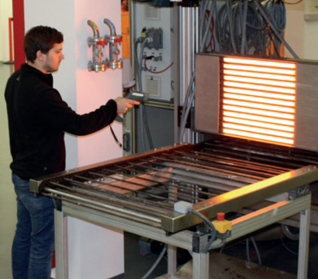
If we’re being honest about hitting carbon neutrality in a semiconductor fab, we have to talk about the energy we’re just tossing away during wafer heating. Most plants are still running on old-school systems that basically act like space heaters for the rest of the room. Switching to short-wave IR lamps helps a lot. But here’s the catch: the actual energy savings come down to one thing. The gap. Specifically, the distance between the lamp filament and the wafer. The physics of that air gap You can’t just throw a lamp into a chassis and call it a day. If the lamp is too far back, you’re wasting heat on the chamber walls. But if you push it too close? You get hot spots. That’s a recipe for warped wafers and thermal stress. We look for a “sweet spot” based on the wattage and how fast you need that temperature to climb. A tighter gap means more heat hits the target faster. It cuts down the total time the power is humming, and that’s where the real carbon wins happen. The trade-off (because nothing is free) More heat density sounds great, but it comes with a price. When you tighten that distance to be more efficient, you’re putting a lot more stress on the lamp’s quartz envelope. If you aren’t careful with your cooling fans or water-jackets, those lamps are going to burn out way too fast. I’ve seen it happen plenty of times. Engineers get so focused on the energy bill that they forget the hardware, and they end up spending all their savings on replacement lamps. What this actually means for your metrics Saving a few seconds per wafer doesn’t sound like much. But when you multiply that by thousands of runs, it’s huge. By dialing in the distance and using precision-coated lamps, you drop the total kilowatt-hours per wafer. It’s probably the fastest way to shrink your carbon footprint without having to rip out and redesign your entire production line.